- 您现在的位置:买卖IC网 > Sheet目录477 > MICRF507YML TR (Micrel Inc)TXRX FSK LOW PWR W/AMP 32MLF
�� �
�
�Micrel,� Inc.�
�MICRF507�
�C5�
�L1�
�Modulation1 Modulation0�
�State�
�ANT� (pin� 5)�
�39pF�
�12nH�
�0�
�0�
�Closed� loop� VCO-modulation�
�0�
�1�
�Not� in� use�
�C4�
�12pF�
�C6�
�12pF�
�1�
�1�
�0�
�1�
�Modulation� by� A,M� and� N�
�Not� in� use�
�Table� 18.� Modulation� Field�
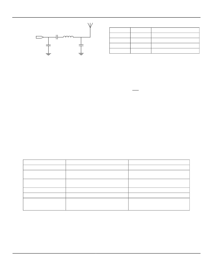
�Figure� 18.� LC� Filter�
�This� filter� is� designed� for� the� 490MHz� band� with� 50?�
�terminations.� Component� values� may� have� to� be� tuned� to�
�compensate� for� layout� parasitics.�
�Bits� from� the� microcontroller� to� be� transmitted� enter� at� the�
�DATAIXO� pin.� See� Table� 19.�
�The� modulation� index� ?� must� be� a� minimum� of� 2.� It� is�
�given� by�
�Frequency� Modulation�
�The� MICRF507� supports� two� methods� of� FSK� modulation,�
�selected� with� the� Modulation� field� as� shown� in� Table� 18:�
�β� =� 2�
�f� DEV�
�r� b�
�VCO� modulation� (enabled� when� Modulation1� is� bit� set� to�
�0)� and� divider� modulation� (Modulation1� bit� set� to� 1).� The�
�Modulation0� bit� must� always� remain� 0.�
�VCO� Modulation�
�in� which� f� DEV� is� the� single-sided� deviation� and� r� b� is� the� bit�
�rate.� Another� constraint� on� f� DEV� is�
�f� DEV� ≥� r� b� +� f� OFFSET�
�where� f� OFFSET� is� the� total� frequency� offset� between� the�
�receiver� and� the� transmitter:�
�The� calculated� f� DEV� should� be� used� to� calculate� the� needed�
�receiver� bandwidth,� see� “Switched� Capacitor� Filter”�
�section.�
�Frequency� Divider� Modulation�
�Set� Modulation[1:0]� to�
�Means� of� modulation�
�Register� fields� to� set�
�PLL� bandwidth� required�
�Bitstream� constraints�
�Instantaneous� frequency�
�waveform� (spectrum)�
�00�
�VCO� modulation� using� modulator�
�Refclk_K,� Mod_clkS,� Mod_I,� Mod_A,�
�Mod_F�
�Lower� than� 1/10� of� bit� rate�
�DC� balance� required�
�Register� fields� affecting� modulator�
�10�
�Divider� modulation� by� switching� between�
�A0/M0/NO� and� A1/M1/N1�
�A0,� M0,� N0,� A1,� M1,� N1�
�Higher� than� 2x� bit� rate�
�None�
�PLL� transient� response�
�determined� by�
�Table� 19.� Modulation� Modes�
�October� 2,� 2013�
�29�
�Revision� 2.2�
�发布紧急采购,3分钟左右您将得到回复。
相关PDF资料
MICRF600DEV1
KIT DEV RADIOWIRE 902-928MHZ
MK01-C
SENSOR REED SPST-NO SMD
MK01-H
SENSOR REED SPDT-CHANGE SMD
MK02/0-1A66-500W
SENSOR REED SPST-NO
MK02/6-0
SENSOR REED PCB 24MM T/H
MK03-1C90C-500W
SENSOR REED SPDT CYLINDER
MK05-1A66C-500W
SENSOR REED SPST-NO SCREW MOUNT
MK06-6-A
SENSOR REED SPST-NO SIL T/H
相关代理商/技术参数
MICRF507YMLTR
制造商:MICREL 制造商全称:Micrel Semiconductor 功能描述:470MHz to 510MHz Low-Power FSK Transceiver with +10dBm Power Amplifier
MICRF507YML-TR
功能描述:IC RF TxRx Only General ISM < 1GHz 470MHz ~ 510MHz 32-VFQFN Exposed Pad, 32-MLF? 制造商:microchip technology 系列:- 包装:剪切带(CT) 零件状态:停产 类型:仅限 TxRx 射频系列/标准:通用 ISM < 1GHz 协议:- 调制:FSK 频率:470MHz ~ 510MHz 数据速率(最大值):200kbps 功率 - 输出:10dBm 灵敏度:-113dBm 存储容量:- 串行接口:SPI GPIO:- 电压 - 电源:2 V ~ 2.5 V 电流 - 接收:8mA ~ 12mA 电流 - 传输:8mA ~ 21.5mA 工作温度:-40°C ~ 85°C 封装/外壳:32-VFQFN 裸露焊盘,32-MLF? 标准包装:1
MICRF600
功能描述:TXRX ISM 902-928MHZ 11.5X14.1MM RoHS:否 类别:RF/IF 和 RFID >> RF 收发器 系列:RadioWire® 产品培训模块:Lead (SnPb) Finish for COTS
Obsolescence Mitigation Program 标准包装:30 系列:- 频率:4.9GHz ~ 5.9GHz 数据传输率 - 最大:54Mbps 调制或协议:* 应用:* 功率 - 输出:-3dBm 灵敏度:- 电源电压:2.7 V ~ 3.6 V 电流 - 接收:* 电流 - 传输:* 数据接口:PCB,表面贴装 存储容量:- 天线连接器:PCB,表面贴装 工作温度:-25°C ~ 85°C 封装/外壳:68-TQFN 裸露焊盘 包装:管件
MICRF600 TR
制造商:Micrel 功能描述:Micrel MICRF600 TR RF Transceivers
MICRF600_06
制造商:MICREL 制造商全称:Micrel Semiconductor 功能描述:902-928MHz ISM Band Transceiver Module
MICRF600DEV1
功能描述:KIT DEV RADIOWIRE 902-928MHZ RoHS:是 类别:RF/IF 和 RFID >> RF 评估和开发套件,板 系列:RadioWire® 标准包装:1 系列:- 类型:GPS 接收器 频率:1575MHz 适用于相关产品:- 已供物品:模块 其它名称:SER3796
MICRF600TR
制造商:MICREL 制造商全称:Micrel Semiconductor 功能描述:902-928MHz ISM Band Transceiver Module
MICRF600Z
功能描述:TXRX ISM 902-928MHZ 11.5X14.1MM RoHS:是 类别:RF/IF 和 RFID >> RF 收发器 系列:RadioWire® 产品培训模块:Lead (SnPb) Finish for COTS
Obsolescence Mitigation Program 标准包装:30 系列:- 频率:4.9GHz ~ 5.9GHz 数据传输率 - 最大:54Mbps 调制或协议:* 应用:* 功率 - 输出:-3dBm 灵敏度:- 电源电压:2.7 V ~ 3.6 V 电流 - 接收:* 电流 - 传输:* 数据接口:PCB,表面贴装 存储容量:- 天线连接器:PCB,表面贴装 工作温度:-25°C ~ 85°C 封装/外壳:68-TQFN 裸露焊盘 包装:管件